We saw the basic functions of the CPU in the last lesson, including the control unit’s role in coordinating the use of the buses to perform the FDE cycle.
The most fundamental signal on the control bus is the clock, which is simply a signal that alternates between 1 and 0 millions of times a second. The rate at which this signal alternates is called the clock speed. The period of time that the signal goes to 1 and then 0 before it switches back to 1 again is called a clock cycle.

Clock speed is significant, because a processor will take a minimum of one clock cycle to execute a single instruction. A more complex instruction could take several clock cycles to execute. Therefore the more clock cycles we can pack into a single second, the more instructions we can execute and the faster our programs will run.
A clock cycle length can be calculated using the following formula:
clock cycle (secs) = 1 / clock speed (hertz)So one aspect of how fast a CPU can execute instructions – which we formally refer to as CPU performance – is clock speed. One early method of comparing different CPUs was to specify how many Millions of Instructions Per Second (MIPS) could be executed by any given CPU.
Activity 1 ( 5 minutes)
Find the clock speeds, and calculate the length of a clock cycle, for each of the following computers/consoles:
- The original IBM PC from 1981
- The original Apple Mac from 1983
- The Nintendo Wii
- The PlayStation 5
Cache
To say that a single instruction can be fetched, decoded and executed in a single clock cycle is a massive simplification. One issue is that the CPU can usually operate at speeds much faster than the memory that it fetches its instructions from.
To improve performance, modern CPUs have very fast memory integrated on the same circuit as the rest of the CPU. This is called cache memory or just cache.
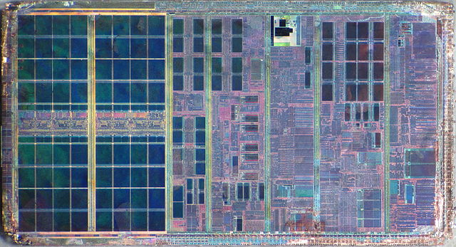
The cache contains instructions (and data) that are used regularly, so the CPU can fetch these items from the fast cache rather than the slow external memory which would necessitate use of the external data and address buses.
How does the cache know which instructions and data to hold? Some sort of algorithm will be deployed to guess which data to hold in the cache. For example an algorithm making use of the 80/20 rule could help determine which parts of memory to hold in the cache. This rule states that 80% of a program’s execution time is spent in 20% of the code. This is not surprising when you think that much of a program’s time will be spent in loops.
When the CPU wants to access memory, it first checks if there is a copy of that memory location in the cache. If it is (called a cache hit), it just fetches the item from the cache. If it is not present (called a cache miss) the CPU will have to fetch the instruction or data from external memory.
Whichever algorithm is deployed to manage the cache takes into account how many cache hits/misses are occuring to determine whether it should try another approach. This whole process is taken care of by hardware inside the CPU so the programmer doesn’t need to worry about it.
Cache is expensive so there will not be much of it inside the CPU. Sometimes there will be differing levels of cache, with different sizes and different speeds, e.g.
- Level 1 cache – fastest but smallest
- Level 2 cache – more capacity than level 1, but not as fast
- Level 3 cache – larger but slower than previous levels of cache
Activity 2 (5 minutes)
Read the article here and write a definition of CPU cache in your notes, and make a note of the sizes of the various levels of cache on a typical modern Intel CPU.
Harvard Architecture
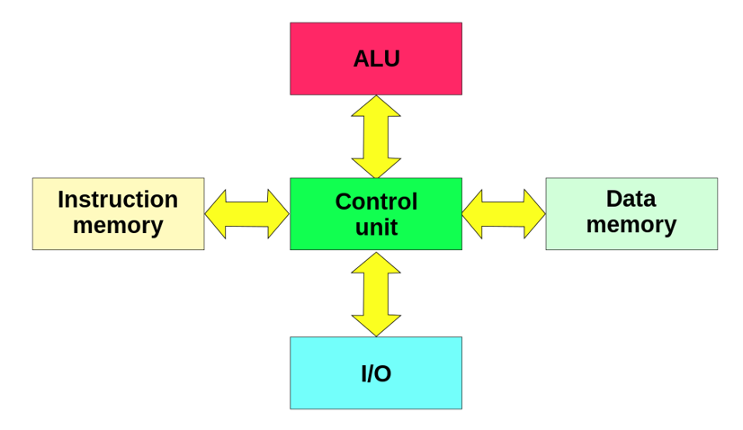
The typical CPU architecture we studied at GCSE and in the previous lesson is the Von Neumann architecture. This is a simple system in which the same memory is used to store both instructions and data. This means that both instructions and data are being sent over the data bus one after the other. An alternative architecture is the Harvard architecture (named after the university).
As the diagram below shows, there are now separate buses and memory for instructions and data. This means an instruction can be fetched on one bus (using the instruction memory data bus and address bus), at the same time as a data is fetched on another (the data memory data bus and address bus). Because instructions and data can be fetched at the same time, the overall performance is quicker than a Von Neumann CPU running at the same clock speed.
This issue with Von Neumann CPUs being slower because they have to fetch instructions and data on the same bus and the CPU is kept waiting while they are fetched, is commonly called the Von Neumann bottleneck.
Harvard architecture is commonly used in systems where multiple data items are fetched and processed simultaneously, for example in special devices called Digital Signal Processors, or in CPUs designed for embedded systems called Microcontrollers. These Microcontrollers often run at very low clock speeds, and contain input and output devices directly on the chip to minimise cost. Harvard architecture compensates slightly for the slower clock speeds to improve performance.
Another advantage of the Harvard architecture over Von Neumann is that it is possible for the data and address buses to be a different size for data memory and instruction memory. This might be useful as generally instruction sets are small, so could for example use an 8 bit data bus, whereas it might be more useful to have data being sent across the data memory data bus as 32 bit values. This would not be possible in Von Neumann as the single address and data bus would have to cope with a single size appropriate for data AND instructions.
Activity 3
Use any sources you can to answer the following questions:
- What is an Arduino?
- What sort of CPU architecture is it?
- What clock speeds do Arduino systems typically use?
- Is this sort of clock speed and architecture sensible for an Arduino? Why?
Contemporary Processor Architectures
Modern CPUs might diverge from the the two classic architectures mentioned above. In particular, neither of those classic designs mention cache memory which is now common. In addition, some of the lines between the two CPUs might have been blurred so we see a hybrid of both architectures in some ways. For example:
- A single memory might hold data and instructions (Von Neumann), but cache memory might be divided into a cache for instructions and a cache for data (Harvard)
- A CPU might have two data buses that access two sets of data in parallel from separate memories, and a third bus to carry instructions.
Multiple Cores and Parallel Systems
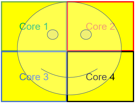
Modern CPUs have come up against physical limitations in making them run at ever faster clock speeds. A solution to increase performance is to use multiple CPUs on a single integrated circuit. Each one of these CPUs is a self contained circuit that can perform the FDE cycle independantly.
This could increase the performance of a system considerably. An example might be an image processing program. On a CPU with 4 cores, the program could instruct each core to process a different part of the image.
However the downside is that the program would have to be specifically written with multicore processors in mind. It is also possible for specially written operating systems to take advantage of multicore systems, the operating system could send different tasks to each core to be executed independently. For example if a web browser had multiple tabs open, each tab could be sent to a different core for execution.
In such specially written software, the cores are processing in parallel hence this is known as parallel processing. Because it is rare to have situations that perfectly lend themselves to parallel processing, and also because there is some overhead involved in the operating system coordinating the activity on the multiple cores, there is not always a significant performance improvement with multicore processors. It might be better to use a single core processor with a higher clock speed and more cache memory.
Activity 5
Abby buys a new computer system which has a multicore CPU, but finds that her old system which only has a single CPU performs better. Explain how this could be possible.
RISC and CISC
The CPUs that were developed in the 1970s and 1980s for microcomputers like the IBM PC, Apple II and Mac made use of an extensive set of machine code instructions. An instruction set is the finite set of all possible instructions that can be executed by any given CPU.
These original CPUs have now retrospectively been named Complex Instruction Set Computers (CISC). We said earlier that it was a simplification to say that each instruction in the FDE cycle is completed in one clock cycle. For CISC CPUs, depending on how complex the instruction is, it might take multiple clock cycles for a single instruction to be executed. It turned out that whilst it was nice to have a large number of machine code instructions to choose from, it increased the complexity of the CPU considerably. To make matters worse some of the instructions in CISC processors were very rarely used.
Another approach was later adopted. This was to use a more restricted set of instructions, giving the advantage that the complexity of the CPU was reduced, and that instructions could be completed in a single clock cycle. This type of architecture was called the Reduced Instruction Set Computer (RISC). This is now the dominant form of CPU as it is used for mobile phones.
Activity 6
Using the article here
- Summarise the difference between RISC and CISC processors
- List the relative advantages and disadvantages of RISC and CISC processors
- Suggest the appropriate use cases for RISC processors and CISC processors
Co-Processors
A co-processor is an extra processor used to provide additional specific functions to the CPU. Not all systems have one, but a common one would be a floating point co-processor (also sometimes called a Floating Point Unit or FPU). This is used to speed up any calculations the CPU does that involve fractional numbers. Arithmetic in the main CPU would be integer based, so having a co-processor that can do hardware based fractional arithmetic is a useful way of improving system performance.
Other types of co-processor might assist with graphics processing, or more general signal processing. Some Intel processors in the 1990s labelled such processors with the acroynm MMX, for MultiMedia eXtensions.
Pipelining (A Level)
GPUs (A Level)
DSP (Extended)
Key Questions
- What is a cache hit?
- What is the Van Neumann bottleneck?
- Why does a multicore processor not always give better performance than a single core processor?
- How do contemporary CPU architectures differ from classic Von Neumman or Harvard architectures?
- What is a co-processor?
- Name one advantage and one disadvantage of RISC over CISC
- How can pipelining improve performance?
- What other uses of a GPU are there apart from graphics?